| ▲ Electronics |

 |
After this page was posted on Hackaday, a commenter pointed out that 7.5V is actually a standard power supply voltage! I never knew this, so I was only searching for 5V, 12V, 24V supplies. Sure enough, there are lots of 7.5V supplies around - for example TRC Electronics. In addition, most of these will have ±5% adjustment so, for the original application which required 7.4V, I could just have used an off-the-shelf supply instead. |
Nearly all Chinese-made power supplies of this type I've come across have had very poor heatsinking of the various power semiconductors - transistors, diodes etc. Little care is taken to ensure good thermal contact with the metal casing, so I always strip the supply down, check the mounting of the heatsinks, and apply some extra thermal grease.
Also, some of the tracks on this supply have insufficient creepage/clearance - see red section further down the page for details.
I'm currently working on a product which uses a size 2430 "hobby" brushless motor and 25A electronic speed controller (ESC). In its "intended" use, the controller runs from two lithium-ion batteries with a total voltage of around 7.4V, but I want to run it from a mains-derived power supply instead. However, there are no off-the-shelf supplies available with that output voltage.
Fortunately, there is no shortage of inexpensive Chinese switchmode supplies with standard outputs of 5,12,24V etc. Most (all?) of these have the ability to adjust the output voltage slightly, by around ±10%. I reckoned that it should be possible to modify such a supply to provide a fully-adjustable output voltage which could be set to the desired 7.4V. This is by no means a novel idea - many people have modified supplies (a common mod is to increase the output to 13.8V, for ham radio use) - but I haven't seen a good operational analysis of these supplies, so it's a good excuse to do some detective work and figure out what makes them tick.
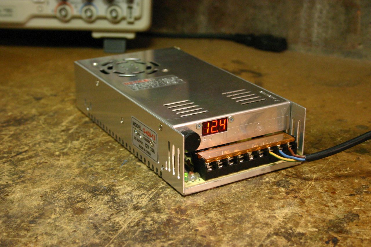
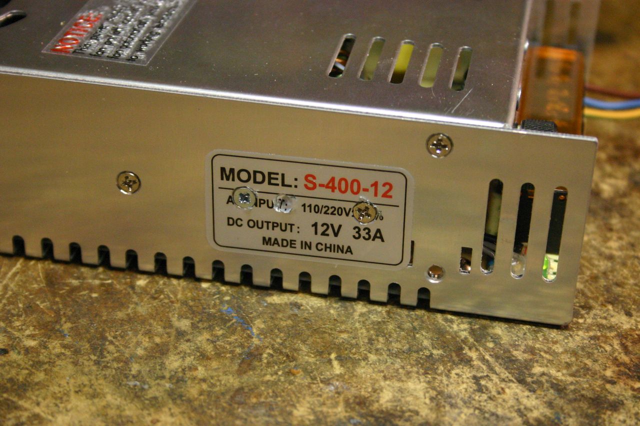
The model numbering scheme for these supplies appears to be S-AAA-BB, where AAA is the power rating in watts and BB is the output voltage. For this application, I've used an S-400-12 supply (400W, 12V, 33A). Here it is:
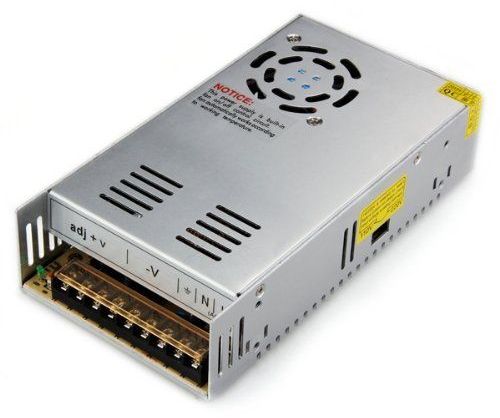
Here is a copy of the original EBay listing. It was very cheap - actually less than some of the 360W supplies which are available! Because of the relatively high power rating, it has a cooling fan which turns on when the power supply's temperature (measured with a thermal switch placed inside the output filter inductor) rises above a certain point.
First task - get the main PCB out, scanned/photographed, traced, and a circuit drawn. My procedure was roughly the following (all processing done in Photoshop):
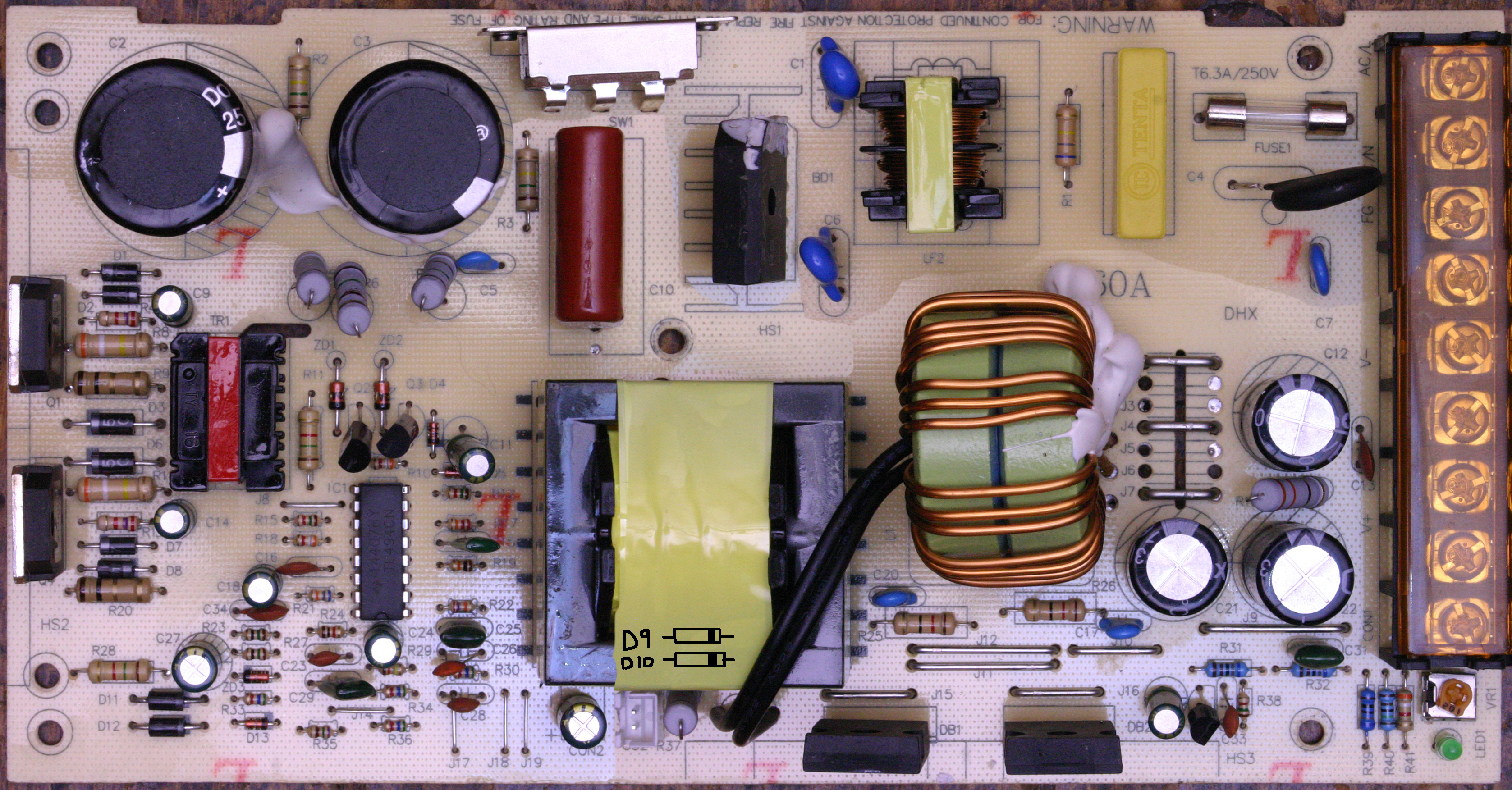
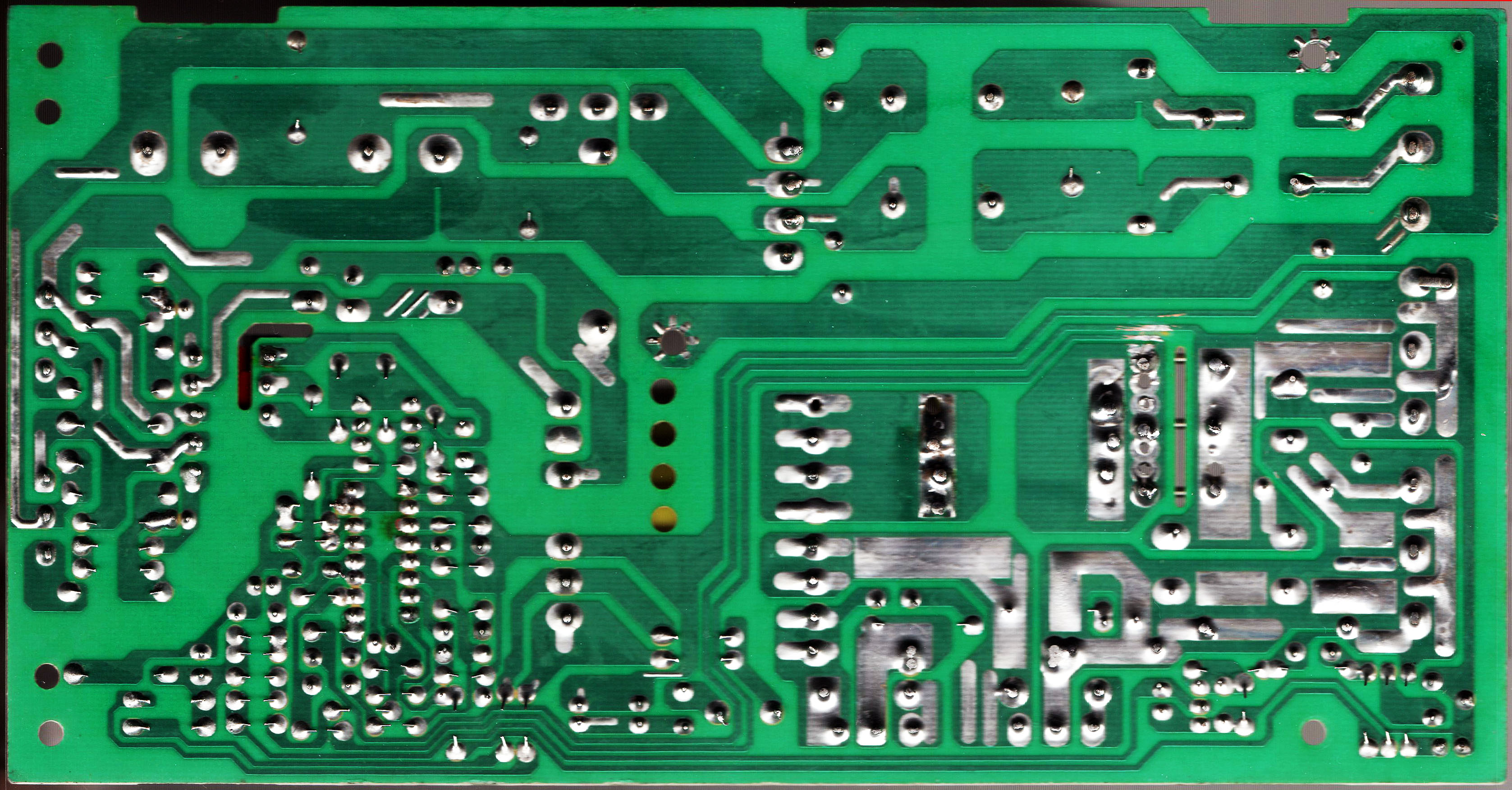
Here's high-res images of the PCB:
 |
 |
 |
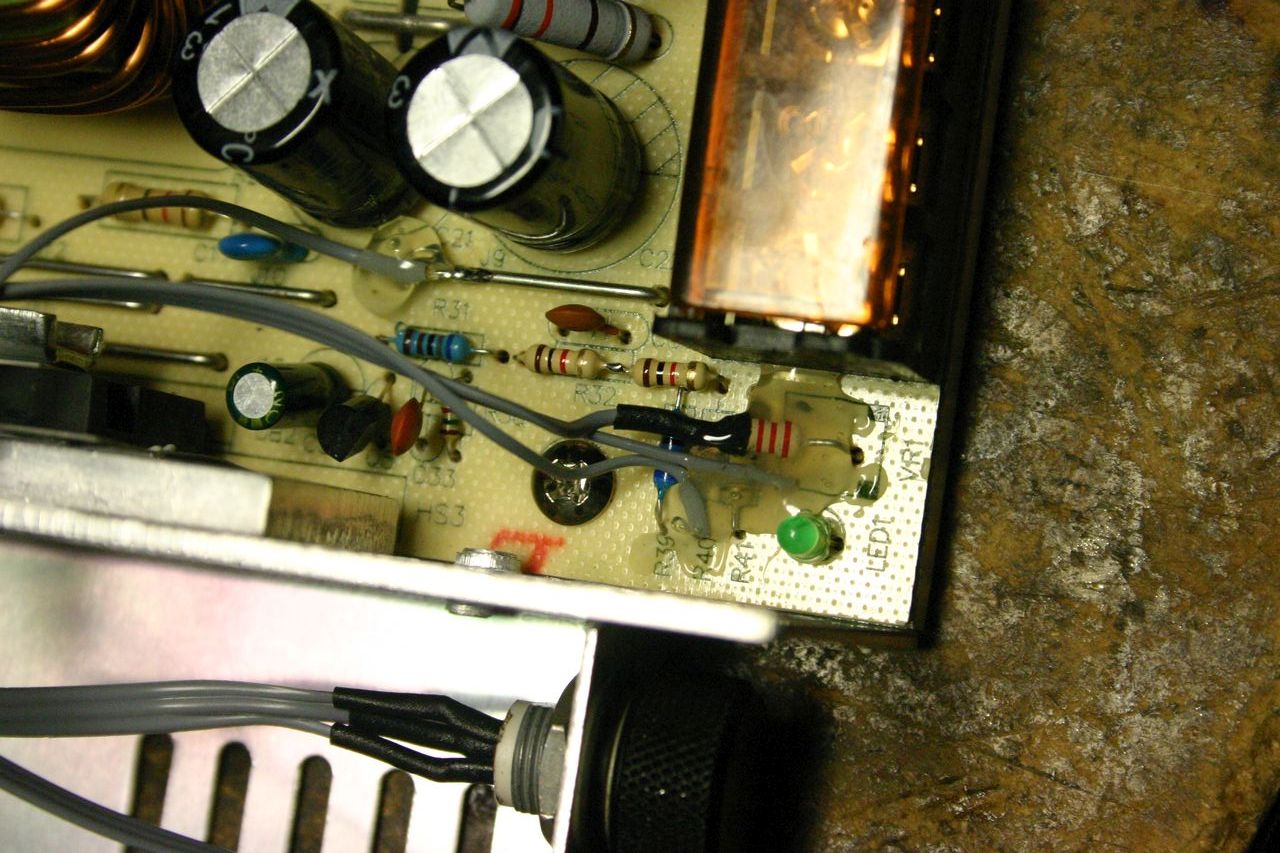
Important note on creepage/clearance: An eagle-eyed reader (RW) pointed out that there is insufficient creepage/clearance between several of the tracks on the PCB. The tracks in question are [ZD2 cathode/Q3 collector/TR1] and [upper ends of R5/R6/R7]. The location, and a possible solution, is highlighted in the image below (tracks viewed from above, looking "through" the PCB). It's just to the right of the L-shaped slot underneath TR1.
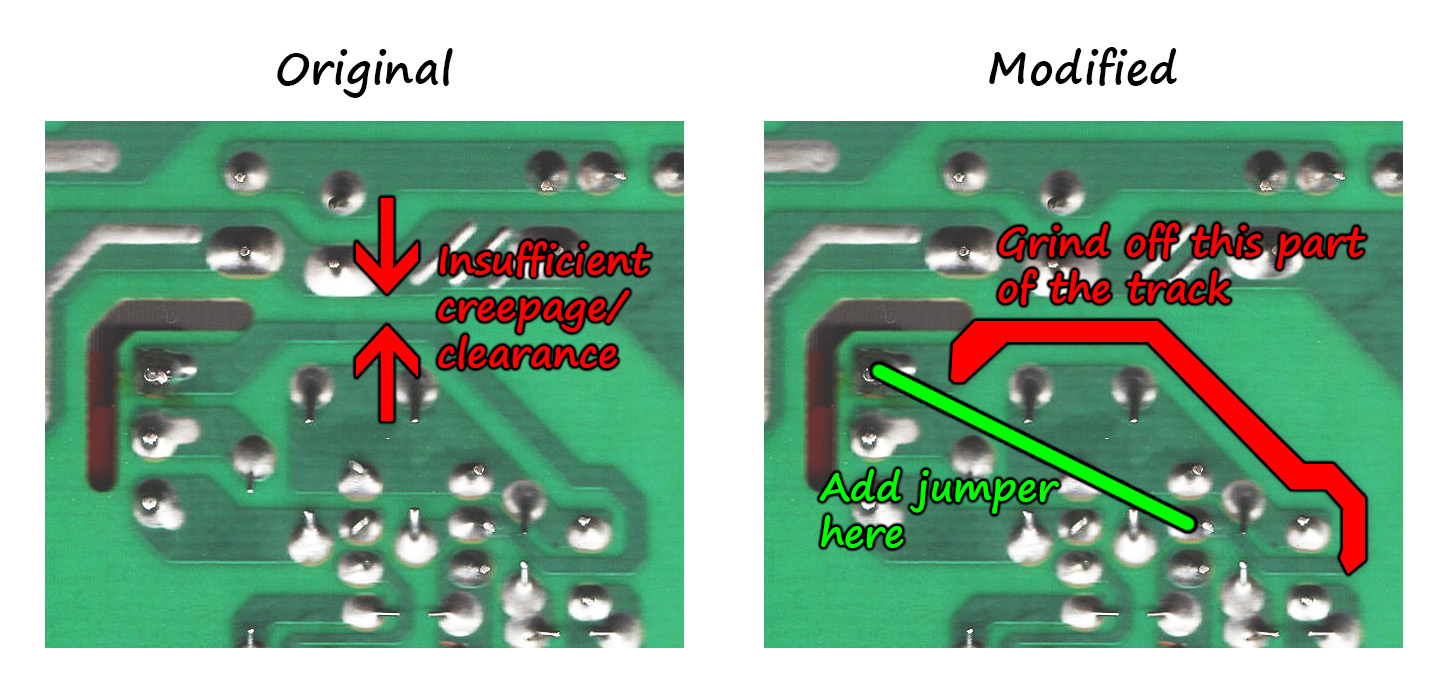
The distance between the tracks is only about 1.5mm which is far less than a safe value (check out these tables of creepage/clearance distances). As shown, a simple solution would be to remove part of the track and re-wire it with a jumper. Ideally, the slot should be extended as well, but there might not be space for that.
In conclusion, it's always worth checking for any creepage/clearance problems in a supply, and making some attempt to correct them, if you value your safety!
And, what you've all been waiting for, the full schematic (click image to link to the PDF). An Eagle schematic is also available here.

I also removed the two transformers and measured their properties (inductance, phasing, ratios, resistance) - click below for a PDF:
It's a pretty standard sort of supply - half-bridge topology, with a single TL494 PWM controller chip running everything. Isolation is provided by the base drive transformer, so there's no need for optocoupler feedback.
I'll go through each main section of the circuit and try to describe its operation. Some sections correspond to the dotted boxes on the circuit diagram, others don't!
This is a pretty bog-standard circuit. Fuse, common-mode choke, filter capacitors to block/absorb any HF interference, the a full-wave bridge rectifier and two smoothing caps. Note that C2 and C3 are in series - this is so the midpoint can be used as a voltage at half the full supply voltage. One end of the transformer's primary goes to here, the other end gets switched between 0V and the full supply voltage, so the primary sees ± half the full supply voltage.
SW1 is the switch to select between 110V/230V operation. For 230V operation, the switch is open, and the voltage across C2+C3 is the peak AC input voltage. For 110V operation, the switch is closed, and the bridge + the two capacitors act as a voltage doubler so the total voltage across C2+C3 is now twice the peak AC input voltage.
(TR1 is the base drive transformer, I've also called it "gate" transformer sometimes. TR2 is the main transformer.)
The two bridge transistors (Q4 & Q1) switch one end of the transformer's primary between 0V and the full DC supply voltage. There is some very clever trickery going on here which I only barely understand. First, the extra resistors such as R14, R13, R8, R4 bias the main transistors on slightly during startup (keep in mind that the auxiliary supply isn't available during startup, so the TL494 isn't running). One transistor will turn on slightly quicker than the other. If you look closely, note that the bottom end of the main transformer's primary isn't connected directly to the midpoint of the two transistors - rather, it goes through a winding on the base drive transformer. As current starts flowing in the main transformer primary, it induces a current in the base transformer windings, one of which will assist the already-on transistor, switching it fully on. Thanks to some resonant and saturation trickery (probably involving C10, in series with the transformer primary), this whole process repeats for the other transistor, and the whole bridge self-oscillates. This will provide enough power to get the auxiliary supply up (it reaches about 10V, but that can vary), and start the TL494 running, at which point it takes over and controls the switching of the bridge transistors.
Another extremely neat feature of this configuration, in addition to the self-starting capability, is that the TL494 doesn't have to provide the full base drive current to the bridge transistors - the base drive current actually comes from the primary current, coupled through the base drive transformer. The drive transistors on the primary of the base transformer simply manage to control which of the main transistors is held on by the primary current.
All that is an extremely loose and incomplete explanation. Fortunately, there is a fantastic page which describes exactly how it does work - Manfred Mornhinweg has a page on building a 13.8V 40A supply and his design uses nearly exactly the same circuit (or rather, the Chinese supply uses the same circuit as he, since his one probably came first!).
Fortunately (2), understanding the actual operation of this part isn't essential to understanding the rest of the supply, so I wouldn't worry about it too much. It Just Works™.
For the main DC output, there's a center-tapped secondary with a couple of power Schottky diodes doing the rectification. Some smoothing caps, indicator LED, and a big filter inductor (L1).
J1,J4,J7 are low-resistance wire jumpers which are used as a current sensing resistor. Since the PCB is designed with different configurations of power supply in mind (voltages and output currents), there are positions for six jumpers - by changing the number of jumpers, the current limit level can be changed to suit different supplies.
There could probably be a bit more in the way of smoothing capacitors on the output, but the ripple isn't too bad. Note that the caps are only 16V, which is pretty close to the maximum adjusted voltage of this supply of nearly 15V. Choosing 25V rated capacitors would probably be better.
Both of these are derived from the center-tapped auxiliary winding on the main transformer. The fan supply is switched with a thermal cutout to power the fan when the supply overheats. The auxiliary supply provides power (Vcc) to the TL494.
The voltage sense divider (dotted box on far left of schematic) results in an adjustment range of about 10-15V with the default component values. The output of the divider (top of C28) is connected to the noninverting input (pin 1) of the #1 opamp in the TL494. The inverting input (pin 2) goes to a fixed 2.5V reference (half of Vref). The TL494 adjusts its output duty cycle to make the output from the divider equal to 2.5V. The components marked "voltage loop compensation" are voodoo and have the effect of reducing feedback gain at higher frequencies. I only vaguely understand loop compensation, but the idea is to try and prevent oscillation or instability in the supply (e.g. when you have a step transient in the load, you want the supply to respond smoothly and not oscillate around for a while). Capacitors C31 and C28 in the voltage divider also perform loop compensation.
Opamp #2 of the TL494 is used for current limiting. The noninverting input (pin 16) is grounded via R24. The inverting input (pin 15) is tied to Vref (5V) by R21, and to the current sense shunt (parallel combination of J1, J4, J7) by R35. The way this works - if no current is flowing in the output, the current sense shunt has no voltage across it, so the voltage appearing at pin 15 of the TL494 will be (750/(750+68k))*5 = 55mV. As current flow increases, the current sense shunt will pull the end of R35 more and more negative until, when the voltage from the shunt reaches -55mV, pin 15 reaches 0V and the #2 opamp output will trip, reducing the PWM duty at the output. This happens with an output current of 55mV/(3.9mR/3)=42A - a little bit higher than the advertised limit of 33A, but I am probably off in my measurement of the current shunt resistances. Several compoments (C29 + R36) are also used to compensate the current limit loop.
Pin 4 of the TL494 is called the dead-time control input and can be used to implement a soft-start feature. C24 is initially discharged, so when power is applied, the DTC pin is held high. This inhibits the output. As C24 gradually charges up (via R19), pin 4 drops in voltage, which slowly decreases the dead time, bringing the output up to its operating level. Pin 4 settles at about 0.4V.
This part of the circuit had me stumped at first - I couldn't see what it was supposed to do! It's a very clever short-circuit protection.
Suppose that the supply is operating normally, with a 12V output. The base of Q5 is fed by a divider from the DC output voltage. Since the divided voltage produced by R38+R31 (which would be about 2.2V) is well above the base-emitter drop of Q5 (0.7V), the transistor is held on, pulling the voltage on C30 low. Given the forward drop of D13, this will have no effect on the voltage at the DTC input. So, in normal operation, this circuit does nothing.
Suppose that the output is suddenly shorted. V+ drops to zero (or very close) which results in Q5 turning off. C30 will now charge up via R33 and ZD3 from the auxiliary supply. (I'm not sure about the purpose of ZD3). Once it reaches a voltage sufficient for D13 to conduct, it will pull up the DTC input and cause the TL494 to shut down.
If the output short is now removed, the output will remain shut down - Q5 remains off, so C30 is charged, holding the DTC pin high. You might wonder how there is still an auxiliary supply available, when the TL494 is shut down - remember the start-up behaviour, with the bridge transistors self-oscillating? The supply goes into this mode again, which is enough to provide an auxiliary supply of about 10V.
The only way to restore power is to switch the entire supply off, wait, and power on again. Which now begs the question, why doesn't the short-circuit protection trigger at power-up? The short answer - thanks to the soft-start circuit, the DTC pin takes sufficiently long to go low that the output voltage has built up enough to keep Q5 conducting (stay tuned for some graphs of this happening).
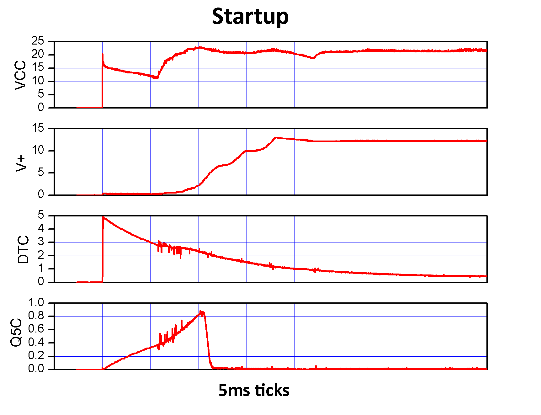
Here's some waveforms when the output is shorted during normal operation. Before shorting, Vcc is about 20V, the output (V+) is 12V, DTC is about 0.4V, and Q5's collector is near 0V - it's being held on by the high output voltage. When the output is shorted, V+ falls to zero. Q5 turns off, and C30 starts to charge up so Q5's collector voltage starts to rise, which in turn causes the DTC voltage to rise. As it rises, the TL494 begins to shut down (dead time increases), until finally the chip is completely disabled, with DTC reaching just under 3V. VCC drops to about 10V since the bridge is now operating in the self-excited mode, as it isn't receiving any drive signals from the TL494.

Next, here's the waveforms during startup with a normal load on the output (i.e. not shorted). On startup, the inverter goes into self-excited operation and VCC immediately goes up to 10-15V or so. DTC immediately jumps high because C24 is initially discharged, and then starts slowly dropping as it charges through R19. Since the output voltage is initially zero, C30 (at Q5's collector) starts charging up via R33. However, as soon as the output voltage builds up to around 3 or 4V (again, thanks to self-excited operation), Q5 is switched on, discharging C30. After this, once DTC falls to a suitable level, normal operation commences. Note that, at all times during normal startup, Q5's collector voltage never reaches DTC plus one diode drop (D13) so the short-circuit protection circuit can never affect the DTC level during normal startup operation.
Lastly, here's the behaviour when the supply is started with the output shorted. The output voltage tries to increase, but can't (since it's shorted). Q5 is held permanently off, so C30 can charge up. Once it reaches a sufficient voltage (DTC + one diode drop), it then holds the DTC pin high, preventing further operation until power is cycled.
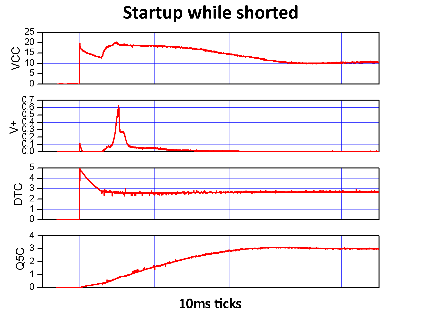
When we're here, an important note regarding the short-circuit protection. Although I've given examples of it tripping in when there's a direct short across the output, it will actually operate whenever the output voltage is insufficient to keep Q5 on - this occurs below about 4V. This means that, when the supply is modified to give a variable output voltage, it isn't possible to reduce the output to below 4V, because the short-circuit protection would kick in. To enable output below 4V, you'd have to disable the short-circuit protection - simplest is to remove D13. However, you then run into another problem - the voltage at pin 2 of the TL494 is held at 2.5V by the R30+R34 divider and it therefore isn't possible to adjust the output below 2.5V. Unless, of course, you changed the values of the divider resistors to produce a different (lower) reference voltage at pin 2, but that's getting more and more involved.
So - on to the modifications!
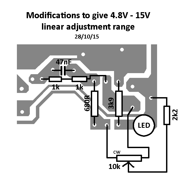
Here is the new feedback divider I've cooked up - this replaces the contents of the dotted box marked "Voltage sense" in the schematic further up the page.
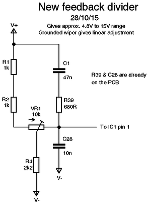
[Note: there is no earthly reason for the two 1kΩ resistors in series - I simply didn't have any 2kΩ resistors in stock!]
There's one important difference between this and the original divider. The original had a very nonlinear adjustment, because VR1 was simply used as a variable resistor between the feedback pin and ground. The new divider has a linear adjustment, thanks to the grounded-wiper configuration. With the values shown, the adjustment is around 4.8-15V; note that I deliberately avoided going too low, to prevent the short-circuit protection kicking in (see earlier). For more details on the advantages of a grounded-wiper feedback configuration, please see this page.
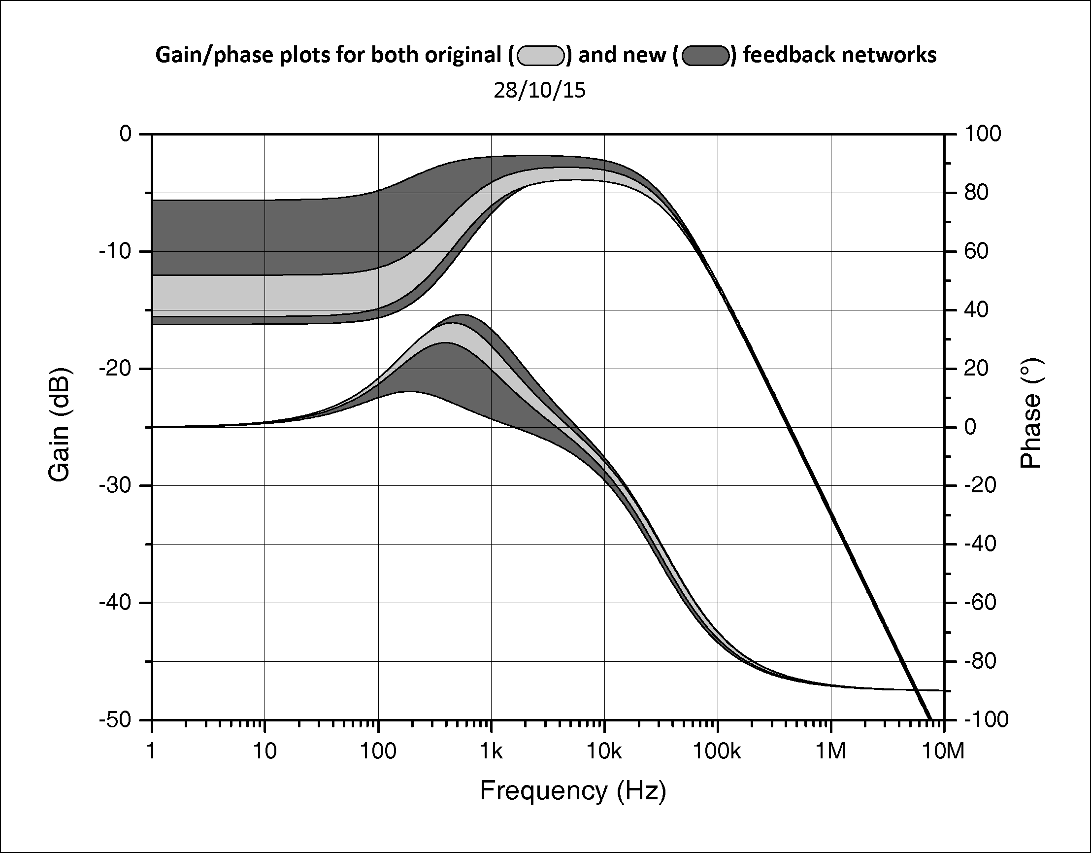
What's with the capacitors? Remember that the original divider had a couple of capacitors in it to provide loop compensation. Now, I really don't know what I'm doing regarding loop compensation, but I reckoned that it would be best to try and get the gain/phase response of the new divider as close as possible to that of the old one, to reduce the chance of any instabilities. I determined the correct component values by trial-and-error in LTSpice. Here's the gain/phase vs. frequency plots for both old and new feedback networks over the full adjustment range - note how, although the range of values is wider for the new divider (thanks to the increased adjustment range), the various corner frequencies are about the same. The boost around 100Hz-10kHz is from C1+R39 coupling more of the output voltage through to the feedback pin, and the drop at high frequencies is from the decreasing impedance of C26.
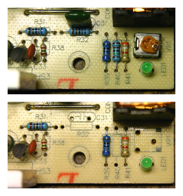
First, remove some of the original components from the PCB. Remove C31, R32, R40, and VR1. Here's a before and after view:
We'll use some of the existing tracks and pads to connect up the components for the new feedback divider. Watch out for the correct orientation for the 10kΩ potentiometer. Here's the layout (viewed from above, looking "through" the PCB):
And that, as they say, is that! The new feedback divider is the only modification needed to give the wider adjustment range - I measured a range of 4.8V to 15V, but it might vary slightly depending on component tolerances. Even at the lowest output voltage of 4.8V, there was no sign of the short-circuit protection kicking in.
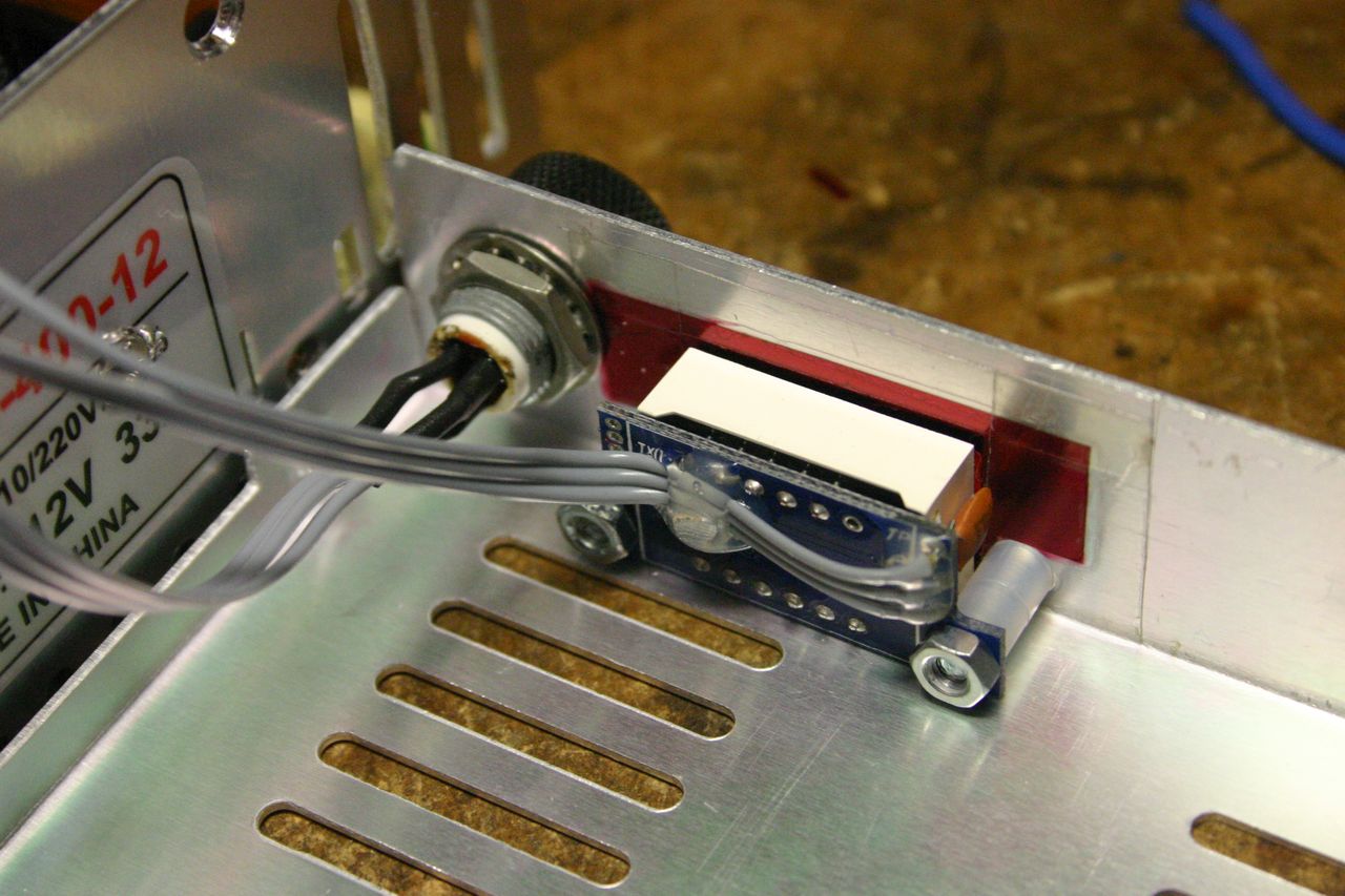
In addition to the voltage divider modifications, I also decided to add a little digital voltmeter module to display the current output voltage. I had bought some meter modules a while back and hadn't found a use for them yet.
Search either AliExpress for TK0600 voltmeter 0-30V or EBay for New 1pcs Digital Voltmeter DC 0-30V Useful LED Panel Meter Red. That's the likeliest search terms to bring up results, but you might have to use a bit of imagination to search for other terms. These particular modules use separate connections for the power supply and the sense, so can measure right down to 0V. Other modules actually run from the sensed voltage, so are limited in how low they can measure. They're neat little modules - 3 digits, automatic decimal point, 0-30V range, and have an onboard STM800S3F3 microcontroller. There's even several I/O pins broken out to a header, so doubtless it could be reprogrammed. Here's a couple of people who have analysed the circuit:
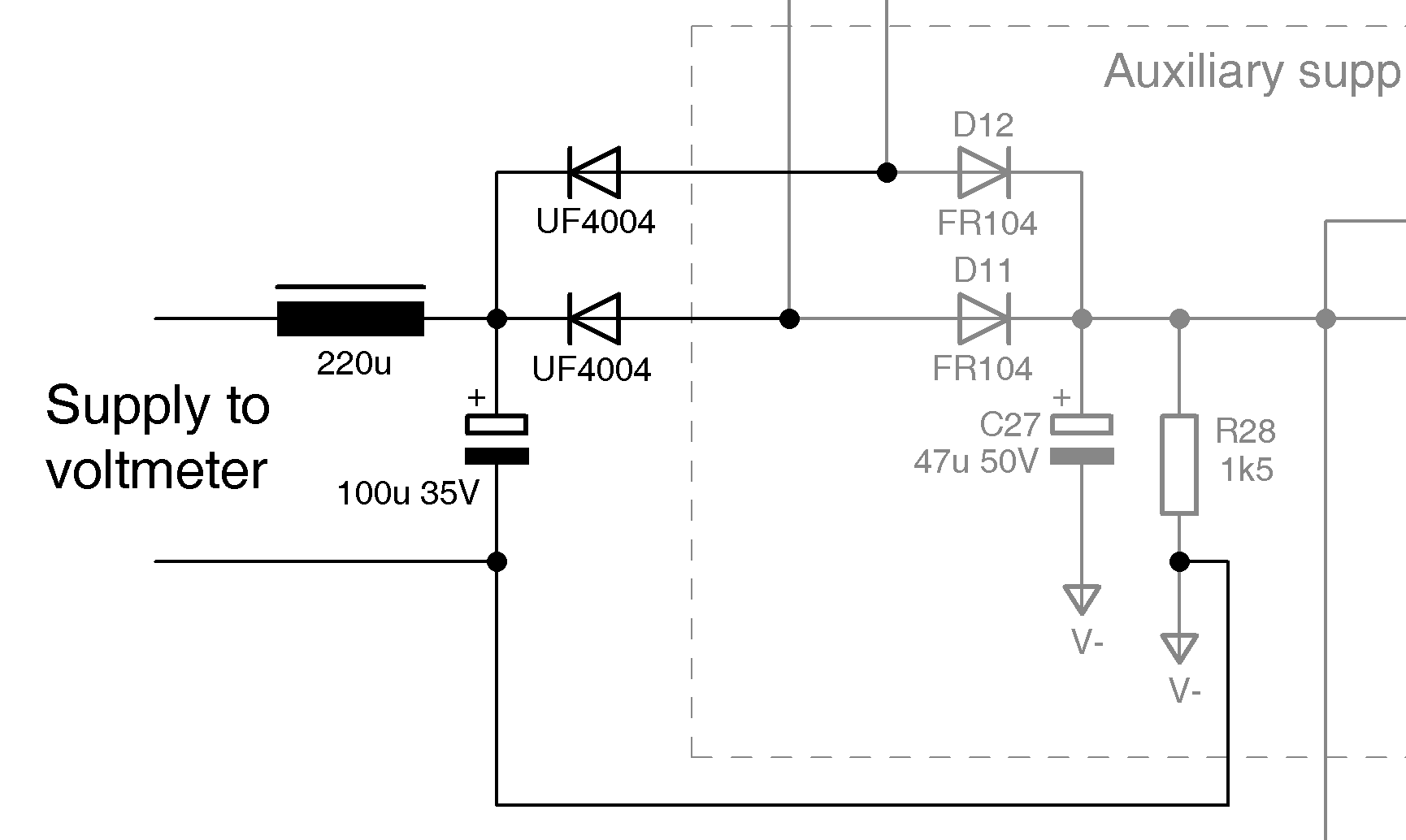
The power supply for the voltmeter module is derived from a couple of extra diodes + 100µF capacitor + 220µH series filter inductor, tacked on to the anodes of D11 & D12 (see photo below). This provides about 20V to the module. According to the EEVBlog posting, the module uses a Holtek 7130 voltage regulator, which has a maximum input voltage of 24V, so this is well within limits. I didn't use the existing auxiliary supply because I found it was a little bit unstable when the supply is operated in a low-load/"self-excited" mode. The voltmeter module's sense connection goes to one of the various big wire jumpers that are used on the output side to increase the current-handling capability of the PCB.
I mounted both the adjustment potentiometer and voltmeter module on the casing of the supply, just above the output terminals. Bit of a squeeze, but there was just enough space to fit them in. I also added a piece of red filter plastic in front of the module to make the display a bit clearer to see.
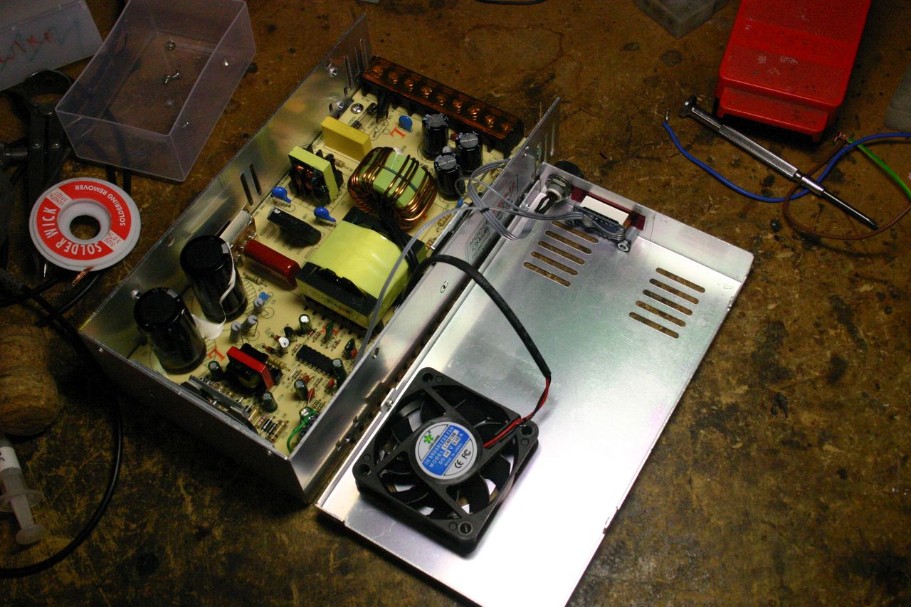 Overall view of the supply's insides |
 New feedback divider connections |
 Power supply for voltmeter module |
 Potentiometer and voltmeter mounted to the case |
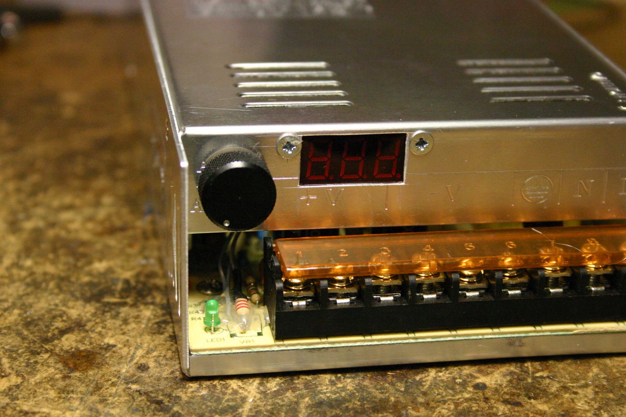 Front view |
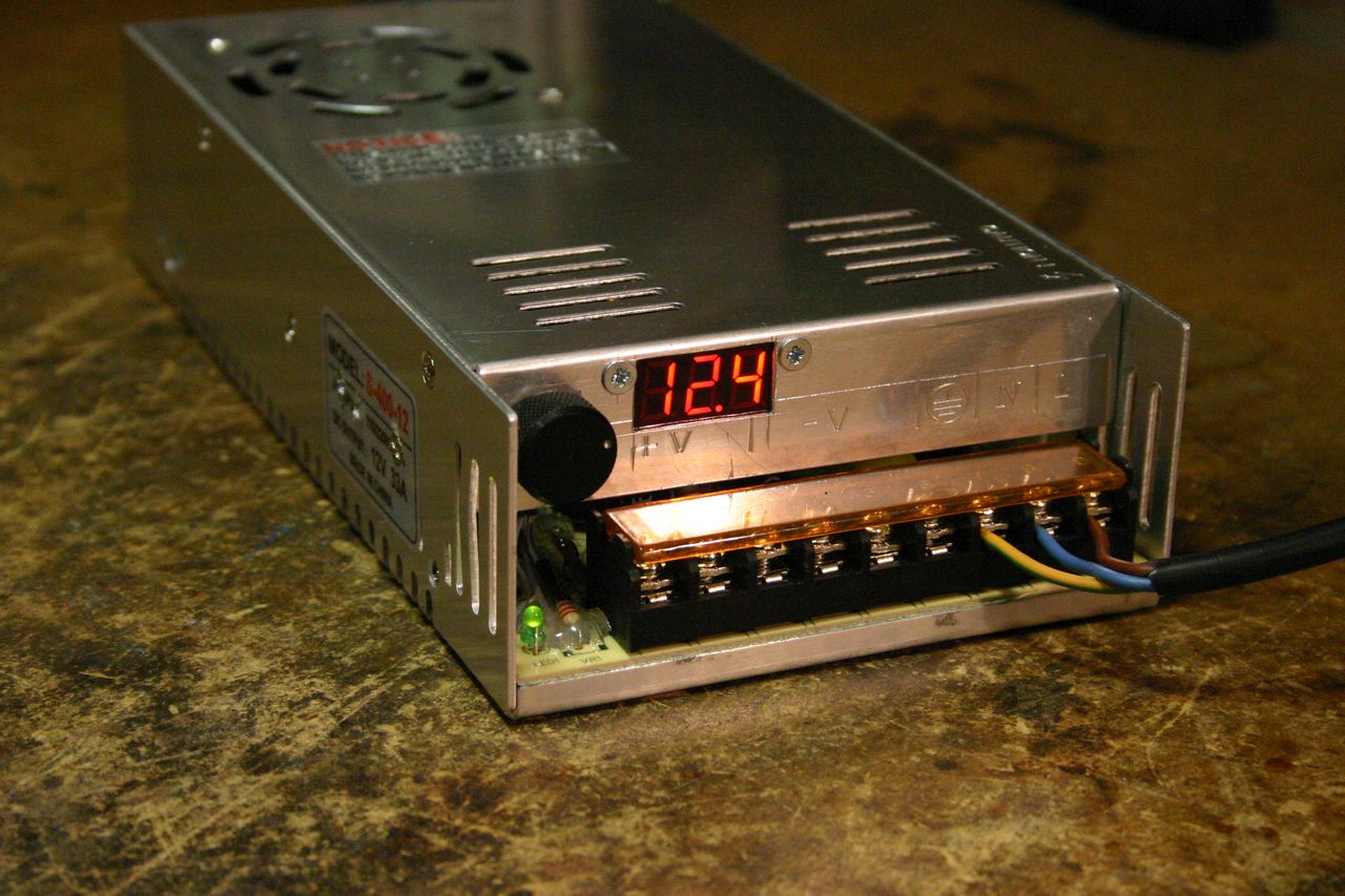 Turned on - the red filter film makes it much easier to see |
 |
 |
The power supply is now adjustable from 4.8V to 15V and appears to work well over the full range. Set to 7.4V, it happily runs the brushless motor; there's a slight drop in voltage at maximum speed, but that's to be expected. I'm using a "servo tester" to provide the adjustable PWM signal to the ESC.
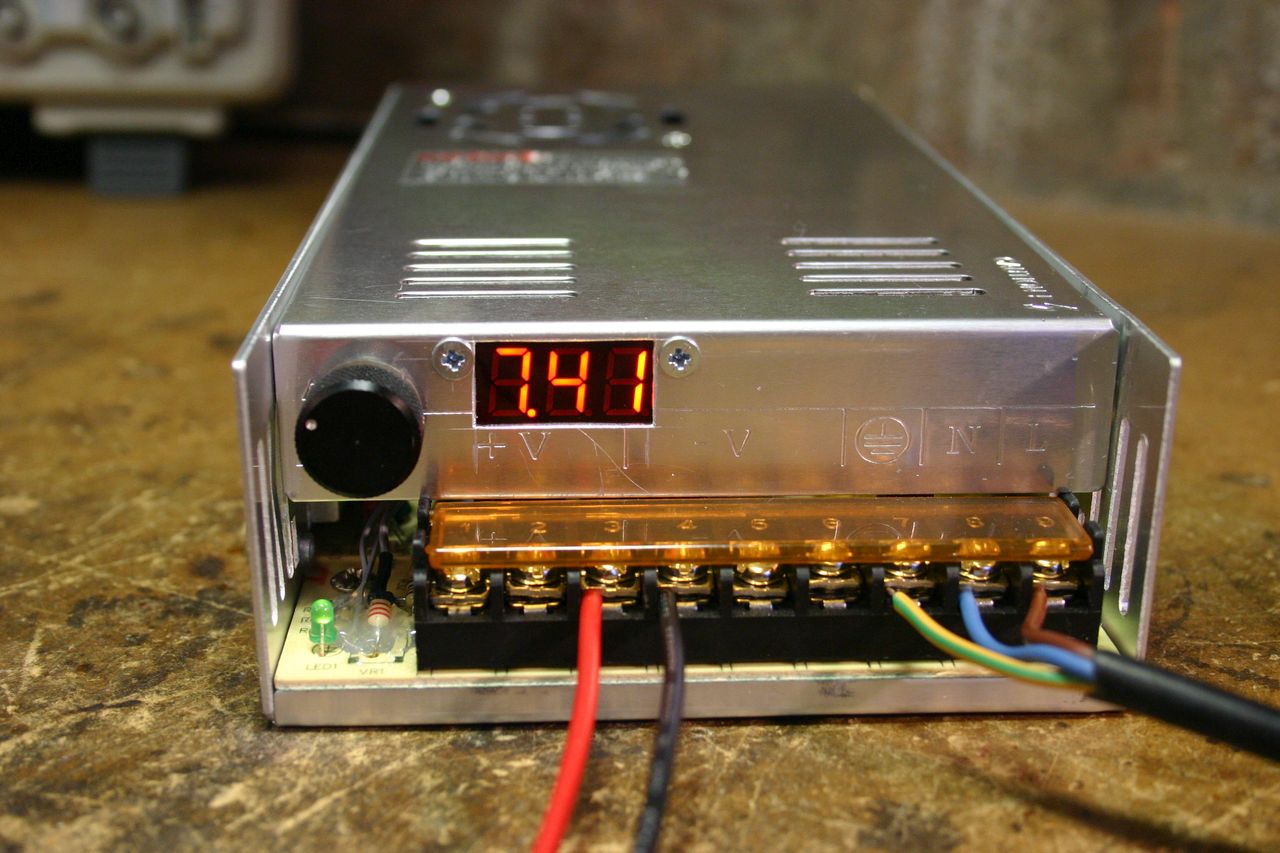 Set to 7.4V for use with brushless motor |
 Connected to 25A ESC and size 2430 brushless motor |
Here's a video overview covering most aspects of the modification:
| ▲ Electronics |